Functional Coating Development
Build repeatable thin films with controlled sputtering
PVD sputtering is a versatile deposition approach for creating thin films with controlled composition, thickness, and microstructure. It is commonly used for conductive, protective, optical, and functional layers where adhesion, uniformity, and reproducibility are key to performance.
In development environments, sputtering is valued for flexible process tuning through parameters such as pressure, power, gas mix, substrate temperature, and cathode configuration. This makes it well suited for iterative optimization across different substrates and target materials. A structured setup helps teams move from exploratory coating trials to stable, repeatable routines that support comparative studies and early-stage application validation.
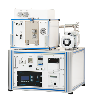
SSP 1000
Laboratory sputtering system (PVD) with sputter‑up/down configurations and planar magnetron cathode (PMC).